We have been reevaluating the strengths and weaknesses of CCD and CMOS looking at the latest generation industrial image sensors and subsequent cameras. We have compared sensitivity, read noise, and blooming and smear performance. Now let’s consider the Modulation Transfer Function or MTF…
The MTF of optics, say a lens, is the reduction in modulation depth, starting with a modulation depth of a hundred percent, due to that optics. The MTF of an optic is usually depicted versus the spatial frequency. Generally speaking the MTF drops with increasing frequency, where frequency is indicated as cycles or line pairs per mm (square-wave signal). In other words, it measures how dependably the lens reproduces (or transfers) details from the object to the image by the lens.
For more background information on MTF and how to measure it, click here.
So while MTF is widely accepted as an important factor with lens selection, it is often not considered with the sensor/camera selection. MTF provides an indication of the sharpness of the image or image quality and is determined by both the lens AND the sensor.
The MTF of the image sensor should not be overlooked when comparing image sensor technologies, especially when working in the Near Infra Red (NIR) spectrum where there are big differences. The MTF of the lens and sensor varies with wavelengths, which can be characterized using MTF-curves. The problem is that sensor manufacturers do not always (read “hardly ever”) specify MTF or when they do, it is only at a wavelength where QE is at maximum value (is close to the best case scenario). The MTF of all sensors at 550 nm is similar, but at longer wavelengths, the MTF of a sensor can be lower compared to other sensors. For some sensors, for instance, the MTF is reduced by a factor of 2 or 3 at 900 nm.
Lower MTF limits the resolution of the system as a result of which small details of objects are no longer discernable, and this is wavelength dependent. In some cases this can be overcome to some extent by decreasing the noise level, which additional to MTF also causes a reduction in contrast, by increasing the light level. The amount of MTF reduction strongly depends on sensor technology:
In the past, CCD technology had better MTF in NIR because of higher electric fields in the depletion layer, and deep-P diffusions for isolation of the columns in the Interline Transfer (IT) structure (compared with standard CMOS pixel design). Until recently, CMOS image sensors used the Shallow Trench Isolation (STI) technique for the electrical isolation between the pixels. Though STI provides a satisfactory electrical isolation between the pixels close to the semiconductor surface (once an electron is captured under the gate of the photodiode it will most likely stay there), there is a significant electrical crosstalk between the pixels.
This crosstalk is caused by the fact that the conversion of photons in electron-hole pairs is taking place at a certain depth in the epi layer – up to several micrometers under the surface of the silicon. At this depth the electrical field strengths are low, and the chance that an electron is stored in an adjacent photodiode is therefore relatively high. This electrical crosstalk results in a poor MTF, and/or poor color fidelity of sensors with a Bayer color filter.

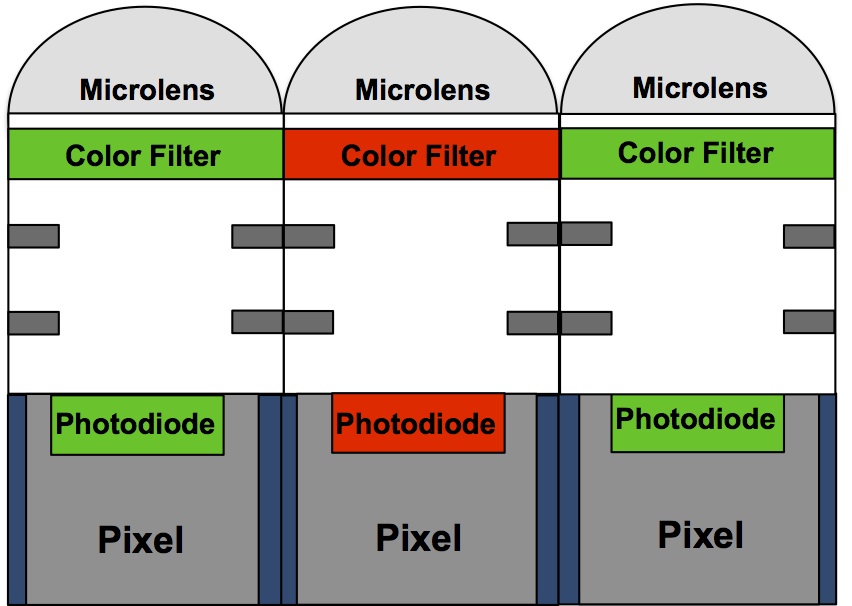
Illustration of Electrical Crosstalk CMOS with Shallow Trench Isolation
The deeper under the surface the electrons are generated, the larger the crosstalk will be. That is the reason why the MTF of a sensor decreases at longer wavelengths. Most CMOS sensors perform therefore poorly in the NIR range. Increasing the QE of a sensor in NIR by using a thicker epitaxial (epi) layer makes this problem even worse.
A typical CMOS sensor MTF at 850 nm (e.g. using a NIR LED or laser illuminator) will be in the range of only 20-30% at Nyquist frequency (is the limiting resolution of the sensor). This is significantly worse than the MTF performance of a state-of-the-art CCD image sensor that reaches approximately 45% under the same conditions.
Modern image sensors use Deep Trench Isolation (DTI) technology to electrically isolate the pixels. DTI was first used in image sensors with very small pixels size (used in cell phones), where electrical crosstalk is a very big problem due to the short distance between the pixels.

Illustration of image sensor with Deep Trench Isolation
The new SONY CMOS image sensor IMX174 however is using DTI in a device with larger pixels and benefits from an excellent MTF in the NIR range. In fact, this CMOS sensor even outperforms the ICX674 CCD from Sony, which has been the golden reference for sensor performance.
Overall with camera selection, be sure to consider the MTF for the full wavelength range or at least for the specific wavelength range in which the camera will be used.
 日本語
日本語 English
 简体中文
简体中文


