 English
 日本語
日本語 简体中文
简体中文CAMERAS FOR SEMICONDUCTOR BACK-END INSPECTION
Cameras for back end semiconductor packaging inspection
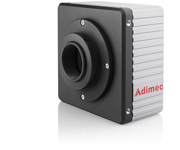 The principle goal of inline optical semiconductor inspection and metrology equipment is to provide 100% analysis at a high precision while maintaining high throughput. But to keep up with the innovations in packaging, the challenges to achieve this drastically increase. The fast-paced progress towards greater densities and finer dimensions are pushing the limits of vision systems. By selecting and utilizing the latest sensor technology, we design cameras that have the required resolution and speed. Driven by getting the best images out of sensors, we ensure predictable and stable equipment operation.
Based on our experience with 2D and 3D measurement methods, we design and tune our products for an exact fit into specific systems.
Cameras for semiconductor metrology and inspection equipment
Our machine vision cameras ensure predictable and stable operation for wafer inspection and metrology equipment.
Optical bump inspection equipment
 Machine vision cameras for optical recognition of:
- Missing bumps
- Bridges
- Nodules
- Bump shapes
- Missing material
Component inspection
 Machine vision cameras for optical 2D/3D inspection of:
- BGA substrates
- Lead frames
- Surfaces
- Marks
- Post dicing
- Packages
Frame rate
To support equipment manufacturers in their challenge to gain throughput we use image sensors with high frame rates. These sensors require a design that can handle these high data rates within a critical timing tolerance to reliably produce quality images.
By our ‘design for quality’ philosophy, we make sure that these frame rates are really captured in a consistent and dependable way!
Field-of- View
Utilizing high-resolution high-speed sensors drives throughput in step-shoot-move inspection systems by both reducing scan time as well as the number of scan positions per object. Uniformity challenges increase as a larger optical field-of- view requires more complex optics and the increase of defects pixels in the sensor.
By grading the incoming sensor, dedicated processing and blemish elimination in our manufacturing process and camera operation, we deliver high resolution images with high uniformity.

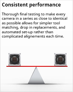
Predictable and stable performance
Consistent images quality over time and cameras.
Repeatability
Images out of a camera vary over time and temperature. Depending on the used measurement method, this may influence the predictability and stability of the inspection system. Using a policy of testing every camera against strict values, we guarantee stable performance of each camera and camera-to-camera.
Reliability
Inline inspection systems benefit from our robust designs. These designs result in highly reliable products and optimize the uptime of the system.
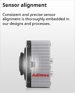
Accuracy
Precise sensor alignment for optimal optical accuracy.
Optical Precision
To achieve high accuracy and precision, particular care has to be given to the optical design and precision of the image sensor placement, especially with high resolution. The alignment of the image sensor in the camera is key to have an optimal optical path. In our camera design and production process, special attention is given to the sensor alignment. This provides the accuracy for the overall system.
Recommended cameras
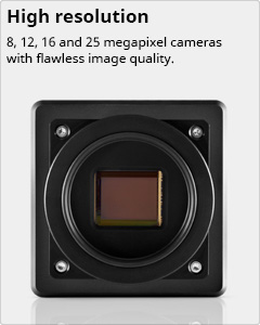
QUARTZ series
Global shutter CMOS
- 5.5 um pixel size
- 2M at 340 fps
- 4M up to 180 fps
- 12M up to 187 fps
- Camera Link, CoaXPress
- 80 x 80 x 29 mm
Norite series
Global Shutter CMOS
- 4.8 μm pixel size
- 5 Megapixel at 105 fps
- CoaXPress at CXP12 speed capability